
01
Broadband design approach
Broadband amplification supports a span of RF signals within a module’s intended operating range. The family offers different design paths; one module should not be assumed to cover every application.
COMPONENT ENGINEERING / RF AMPLIFICATION
Module-level RF amplification for communications, laboratory testing and industrial research. Explore the product family, understand GaN and LDMOS technology paths, and discuss a configuration around your system.
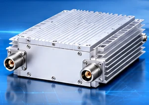
RF MODULES / MODEL SELECTION
Browse 22 reference entries and open each independent model page. The reference numbers preserve the supplied list's order; they are not confirmed commercial model codes.
| Reference model | Frequency reference | Bandwidth reference | Power reference | Transistor technology | RF connector | Weight reference | Dimensions reference | Record status | Details |
|---|---|---|---|---|---|---|---|---|---|
| Reference model 01 | 5–6 GHz | 1 GHz | 10-30 W | GaN | SMA → SMA | 273 g | 132 × 53 × 18 mm | Recorded fields | View model details |
| Reference model 02 | 1.2 GHz 1.5 GHz 2.4 GHz | Lower-band bandwidth200 MHz (e.g.700–900 MHz) Upper-band bandwidth300 MHz (e.g.2–2.3 GHz) | 50 W | LDMOS | SMA → N | 556 g | 179.6 × 66.91 × 22 mm | Recorded fields | View model details |
| Reference model 03 | 3–4 GHz 4–5 GHz 5–6 GHz 3–6 GHz | Bandwidth1 GHz Bandwidth3 GHz | 50 W | GaN | SMA → N | Not provided — confirm | 203.5 × 90 × 24 mm | Confirmation required | View model details |
| Reference model 04 | 100–1000 MHz | Bandwidth1 GHz | 100 W | LDMOS (new revision) | SMA → N | 1020 g | 175.5 × 100 × 24 mm | Recorded fields | View model details |
| Reference model 05 | 1–2 GHz 2–3 GHz 1–3 GHz | Bandwidth1 GHz Bandwidth3 GHz | 100 W | GaN | SMA → N | 1048 g | 200.5 × 105 × 24 mm | Recorded fields | View model details |
| Reference model 06 | Conflicting records — confirm
| Conflicting records — confirm
| 100 W | GaN | SMA → N | 700 g | 175 × 84 × 24 mm | Confirmation required | View model details |
| Reference model 07 | Conflicting records — confirm
| Conflicting records — confirm
| 30 W | GaN | SMA → SMA | 295 g | 160 × 50 × 20 mm | Confirmation required | View model details |
| Reference model 08 | 100–1000 MHz 1–3 GHz Revision 2 | Notation requires confirmation
| 30 W | GaN | SMA → SMA | 396 g | 162.65 × 52.5 × 20 mm | Confirmation required | View model details |
| Reference model 09 | 3–6 GHz | 1 GHz / 2 GHz / 3 GHz | 30-40 W | GaN | SMA → SMA | 294 g | 160 × 50 × 19 mm | Confirmation required | View model details |
| Reference model 10 | 100 MHz-2.4 GHz | Bandwidth300–400 MHz | 50 W | GaN | SMA → N | 425 g | 155 × 58 × 22 mm | Recorded fields | View model details |
| Reference model 11 | Conflicting records — confirm
| Conflicting records — confirm
| Conflicting records — confirm
| GaN | SMA → N | 1351 g | 220 × 110 × 26 mm | Confirmation required | View model details |
| Reference model 12 | 300 MHz-2 GHz Revision 2 | 1.7 GHz | 100 W | GaN | SMA → N | Not provided — confirm | 240 × 118 × 25 mm | Confirmation required | View model details |
| Reference model 13 | Notation requires confirmation
| 900 MHz | Conflicting records — confirm
| GaN | SMA → N | 880 g | 200 × 100 × 20 mm | Confirmation required | View model details |
| Reference model 14 | 1–2 GHz | Bandwidth1 GHz | 80 W | GaN | SMA → SMA | 724 g | 200 × 100 × 20 mm | Confirmation required | View model details |
| Reference model 15 | 1–6 GHz 1–6.2 GHz Revision 2 power claim requires validation | Bandwidth5 GHz | 100 W | GaN | SMA → N | 1830 g | 250 × 150 × 25 mm | Confirmation required | View model details |
| Reference model 16 | 4–8 GHz Revision 2 | 4 GHz | 50 W | GaN | SMA → SMA | Conflicting records — confirm
| Conflicting records — confirm
| Confirmation required | View model details |
| Reference model 17 | 1–3 GHz | 2 GHz | 50 W | GaN | SMA → N | 977 g | 220 × 77 × 24 mm | Confirmation required | View model details |
| Reference model 18 | Conflicting records — confirm
| Not provided — confirm | Variant rating requires confirmation
| GaN | SMA → SMA silver-plated connectors | 278 g | 105 × 60 × 20 mm | Confirmation required | View model details |
| Reference model 19 | 4–8 GHz | 4 GHz | 100 W | GaN | Conflicting records — confirm
| 1193 g | 160 × 160 × 25 mm | Confirmation required | View model details |
| Reference model 20 | 2–7.2 GHz | 5.2 GHz | 50 W | GaN | Conflicting records — confirm
| Not provided — confirm | 160 × 160 × 25 mm | Confirmation required | View model details |
| Reference model 21 | 2–7.2 GHz | 5.2 GHz | 100 W | GaN | SMA → SMA | 2569 g | 240 × 220 × 25 mm | Recorded fields | View model details |
| Reference model 22 | Notation requires confirmation
| Conflicting records — confirm
| Conflicting records — confirm
| GaN | N | 778 g | 226 × 74 × 22 mm | Confirmation required | View model details |
For lawful civilian communications, laboratory equipment and industrial research. These records are not installation instructions, interference settings, a safety assessment or a certification claim. The original workbook and internal engineering notes are not public downloads.
01 / THE MODULE APPROACH
An RF power amplifier increases the power of an incoming radio-frequency signal. A module packages that amplification stage for integration into a larger piece of equipment, rather than replacing the complete system.
Broadband amplification supports a span of RF signals within a module’s intended operating range. The family offers different design paths; one module should not be assumed to cover every application.
GaN and LDMOS provide different foundations for an amplifier design. The useful comparison is how the complete module fits the intended signal and equipment—not the semiconductor name alone.
The module format brings the amplifier into a defined physical assembly. Enclosure layout, connection access and the host equipment’s mechanical arrangement are practical parts of a product discussion.
Start with the civilian use case and the surrounding equipment. Discuss mechanical fit, interface arrangements and the support needed to turn an initial concept into an agreed project scope.
02 / PRODUCT FAMILY
The product family brings together several enclosure shapes and connection layouts. Explore the physical formats as a starting point for engineering and purchasing discussions.

Different enclosure proportions can suit different equipment layouts.
Interface placement is a distinct part of each module’s integration context.
Use the family as a starting point, then discuss a specific assembly with the team.
03 / TECHNOLOGY OPTIONS
GaN and LDMOS refer to the transistor technology inside an amplifier. Neither label, on its own, describes the performance of a finished module.
Gallium nitride
A compound-semiconductor technology used in RF power devices. It is often considered where compact RF power stages and broadband design are important to the equipment concept.
Laterally diffused metal-oxide-semiconductor
A silicon transistor technology with a long-established role in RF amplification. It offers another design path for communications equipment and other RF systems.
Compare complete module designs in the context of your application; technology labels are not a universal ranking.
04 / CIVILIAN APPLICATIONS
Three civilian contexts in which a dedicated RF amplification stage can be part of the wider equipment design.
RF amplification within communications equipment and wireless development platforms. A module can form one stage of a transmit chain, alongside the equipment’s other signal-handling components.
Amplification of laboratory signal sources for RF experiments and equipment evaluation. The amplifier belongs within the lab’s complete measurement setup and test plan.
RF subsystems for industrial instrumentation research and prototype equipment. Module-level packaging lets teams consider the amplifier alongside the wider mechanical and electronic assembly.
05 / CUSTOMIZATION SCOPE
Customization starts with understanding the host product and the purpose of its RF stage. These are the areas to bring into an initial discussion with New Ark.
Module-specific enclosure, interface and support arrangements are confirmed in the written project scope.
06 / COMMON QUESTIONS
This category covers amplifier modules intended to become part of larger equipment. An enclosure does not make a module a complete laboratory instrument or communications system; the surrounding equipment and integration responsibilities still matter.
GaN means gallium nitride; LDMOS means laterally diffused metal-oxide-semiconductor. They are different transistor technologies used in RF power amplification. A suitable choice depends on the complete module design and application, rather than one technology being universally better.
No. An RF power amplifier needs an external electrical supply and is an active electronic device. The word “passive” does not correctly describe powered amplification, even if a module has no extra control or monitoring features.
Start with your civilian application, the module’s role in your equipment, the available mechanical space and the interface or documentation questions you want to resolve. The custom project team can coordinate the next review; the agreed configuration and support belong in the written scope.
07 / CONSULTATION
Choose a contact based on what you need to discuss. All three links open WhatsApp directly—no registration or enquiry form required.
Product-family enquiries, quotations and commercial discussions.
+86 19928199130Message salesModule questions, product documentation and technical clarification.
+86 18123677761Message technical supportA project-specific discussion about mechanical fit, interfaces and support scope.
+85295658748Message the project team